CO-Assignment-2
For the following transistor-level circuit, fill in the truth table. What is the logical expression of Z in terms of A and B? (12 points)
Fibonacci numbers are the sequence of numbers Fn defined by the linear recurrence equation
- Truth Table
| 0 | 0 | 0 | 0 | 1 |
| 0 | 0 | 0 | 1 | 1 |
| 0 | 0 | 1 | 0 | 1 |
| 0 | 0 | 1 | 1 | 1 |
| 0 | 1 | 0 | 0 | 0 |
| 0 | 1 | 0 | 1 | 1 |
| 0 | 1 | 1 | 0 | 0 |
| 0 | 1 | 1 | 1 | 0 |
| 1 | 0 | 0 | 0 | 1 |
| 1 | 0 | 0 | 1 | 0 |
| 1 | 0 | 1 | 0 | 0 |
| 1 | 0 | 1 | 1 | 0 |
| 1 | 1 | 0 | 0 | 0 |
| 1 | 1 | 0 | 1 | 1 |
| 1 | 1 | 1 | 0 | 0¡¡ |
| 1 | 1 | 1 | 1 | 0 |
- Sum of Product
- Simplify the logical expression using logical identities
- Simplify the logical expression using K-MAP.

- Draw the logical circuit and verify it.

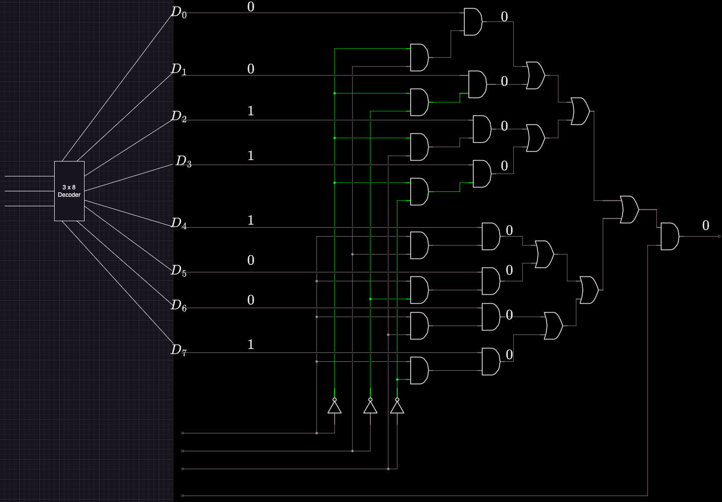
Draw a combinational logic circuit of an eight-input multiplexor where the inputs (D7, D6, D5, D4, D3, D2, D1, D0) are each one-bit variables. Label the values of inputs and outputs of each gate of the circuit, assuming the eight inputs have the values (1, 0, 0, 1, 1, 1, 0, 0) respectively, and assuming D1 is selected. [Note: Assume you have an 3-8 decoder to use as a black box and do not draw the decoder circuit which is part of the multiplexor.] (8 points)
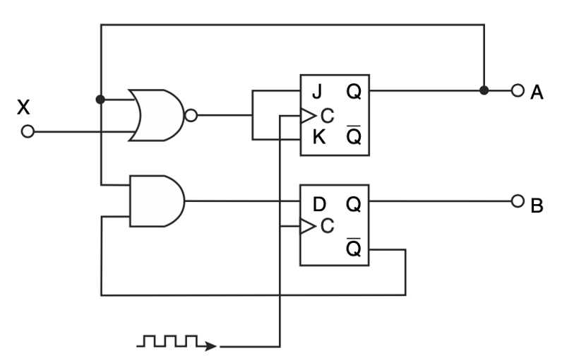
Investigate the operation of the following circuit. Assume the initial state is 0000. Trace the outputs (the Qs) as the clock ticks and determine the purpose of the circuit. You must show your trace to complete your answer. (10 points) 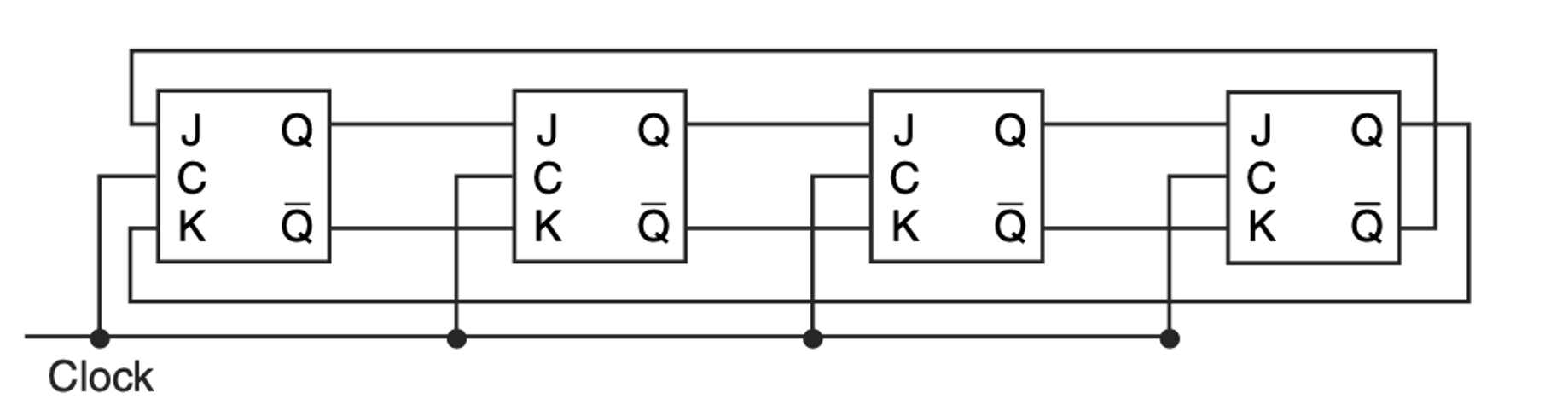
- Equation
Clock equation
Dirve equation
State equation
- Feature equation:
- Feature equation:
- State
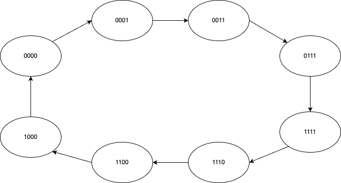 This state diagram describes the function of a four-bit binary right-cycling shifter.
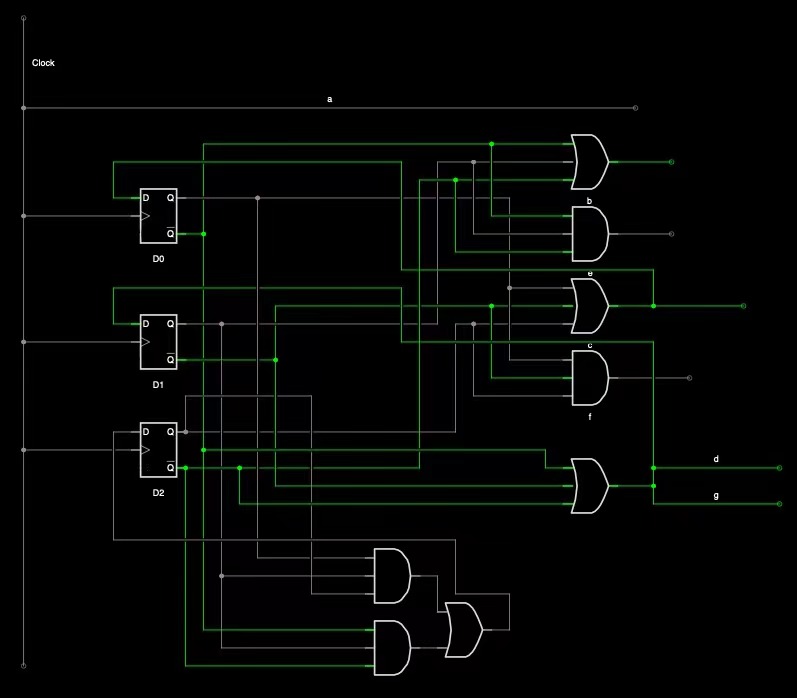
Complete the truth table for the following sequential circuit: (8 points)
| 0 | 0 | 0 | 1 | 0 |
| 0 | 0 | 1 | 0 | 0 |
| 0 | 1 | 0 | 1 | 0 |
| 0 | 1 | 1 | 0 | 0 |
| 1 | 0 | 0 | 1 | 1 |
| 1 | 0 | 1 | 1 | 1 |
| 1 | 1 | 0 | 1 | 0 |
| 1 | 1 | 1 | 1 | 0 |
Design a finite state machine (FSM) for a counter that counts through the 3-bit prime numbers downwards and loop:
- You need to provide the state transition diagram. Assume that the state is stored in three D Flip Flops. Hint: The set of all 3-bit prime numbers includes 2, 3, 5 and 7. (4 points)
- State Diagram

- Design the sequential circuit for the counter. The circuit is driven by the clock. The output is a 7 segment LED display. The various digits from 0 through 9 can be displayed using a 7-segment display as shown in the following figure.