From-Gates-to-Circuits-I-Combinational-Circuits
Basic Building Blocks 基本构造模块
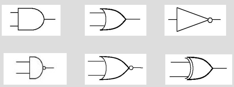
- AND/NAND
- OR/NOR/XOR
- NOT
3 representations logically equivalent to one another
- Truth table
- Logic expression
- Logic circuit
Integrated Circuits (IC)
The integration of large numbers of tiny transistors into a small chip
- Two Types of Circuits
- Combinational logic circuits 组合逻辑电路
- Sequential logic circuits 时序逻辑电路
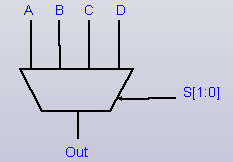
Combinational Circuit
- Circuit with no memory 无内存
- Multiple inputs, multiple outputs, one Boolean function for each output
- Abstracted as a package or a black box 可抽象成黑箱
- Implementation described by one of
- n-input-, m-output-column truth table
- boolean function for each output variable
- logic diagram (possibly using other packages)
Half Adder 半加器
Only add two single bits together (a, b), s is the sum and c is the carry bit 仅实现两个单bit二进制加法

Half Adder: 半加器用于对两个单比特(二进制位)进行加法运算,产生两个输出结果:和(Sum)和进位(Carry)。 - 输入:两个待相加的二进制位
Full Adder 全加器

Full Adder: 全加器用于对三个单比特(二进制位)进行加法运算,包括两个输入位(A和B)和上一位的进位(Cin),产生两个输出结果:和(Sum)和新的进位(Carry)。 - 输入:三个待相加的二进制位(A、B和Cin)。 - 输出: - 和(Sum):(A ⊕ B) ⊕ Cin,即当前位相加的结果,考虑了上一位的进位。 - 进位(Carry):(A ∧ B) ∨ ((A ⊕ B) ∧ Cin),表示下一位相加是否产生进位,综合考虑了当前位和上一位的进位。
- 半加器处理两个输入位的加法运算,产生Sum和Carry
- 全加器处理三个输入位的加法运算,产生 和(Sum)和新的进位(Carry),能够考虑前一位的进位情况
4-bit Adder 连锁进位加法器

feeding the Carry Out of one circuit into the Carry In of the circuit immediately to its left
"Ripple-Carry Adder"(连锁进位加法器)之所以被称为这个名称,是因为它的进位传递机制类似于水波纹在水面扩散的方式。它是一种最基本的加法器设计,用于将两个二进制数字相加。
在Ripple-Carry Adder中,当两个二进制数字的每一位相加后产生进位时,这个进位会向下一位的相加操作传递。这个传递的过程就像水波纹在水面扩散一样,从一位传递到下一位,依次传递到最高位。这一连串的进位传递是串行进行的,因此它的名字中包含了"Ripple"这个词。
Decoder
A decoder uses the inputs and their respective values to select one specific output line.
inputs to a maximum of outputs 个输入最多可以有 个输出
All memory addresses in a computer are specified as binary numbers. When a memory address is referenced (whether for reading or forwriting), the computer first has to determine the actual address. Decoder(译为解码器)是数字电路中的一个常见组件,它用于将输入的编码信号转换成特定的输出信号,根据输入信号的不同编码,Decoder产生不同的输出信号。Decoder有多种用途,包括:
控制逻辑:Decoder用于生成控制信号,这些信号用于控制其他数字电路的操作。例如,它可以用于选择特定的操作模式,启用或禁用特定功能等。
地址解码:在微处理器和微控制器中,Decoder用于解码指令地址,以确定下一步执行的指令或操作。
Decoder是数字电路中的一种重要元件,用于将输入信号从一种编码形式转换为另一种有意义的输出信号,从而实现数据选择、控制、解码和路由等功能。
A 2-4 Decoder
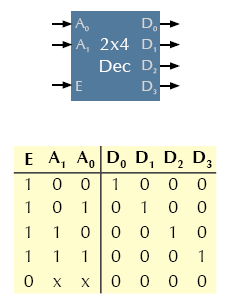
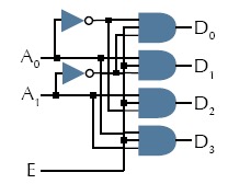
2-4 Decoder(也称为2输入4输出解码器)是一种特定类型的解码器,它具有两个输入线和四个输出线。它的主要功能是将两个输入线的组合编码映射到四个输出线,其中每个输入组合对应一个输出线。
一般情况下,2-4 Decoder的真值表如下:
| 输入(A1, A0) | 输出 D1 | 输出 D2 | 输出 D3 | 输出 D4 |
|---|---|---|---|---|
| 00 | 1 | 0 | 0 | 0 |
| 01 | 0 | 1 | 0 | 0 |
| 10 | 0 | 0 | 1 | 0 |
| 11 | 0 | 0 | 0 | 1 |
Multiplexer
- A multiplexer behaves like a channel selector
- It selects a single output from several inputs.
- The particular input chosen for output is determined by the value of the multiplexer's control lines.
- To be able to select among n inputs, log2 n control lines are needed
- 多个输入一个输出 由控制线路选择选择输出线路
4-to-1 Multiplexer
4-to-1 Multiplexer(四选一多路器)是数字电路中的一个常见组件,用于从多个输入信号中选择一个输出信号。它有四个数据输入(通常称为I0、I1、I2和I3),两个控制输入(通常称为S0和S1),一个电源开关(E),一个输出(通常称为Y)。
4-to-1 Multiplexer的运行原理如下:
控制输入:S1和S0是控制输入,它们确定要从哪一个数据输入传递到输出。这两个控制线有四种可能的组合:00、01、10和11,分别对应着选择I0、I1、I2和I3作为输出。
数据输入:有四个数据输入(I0、I1、I2和I3),每个数据输入上都可以连接一个不同的输入信号。
输出:根据S1和S0的状态,Multiplexer会选择一个数据输入作为输出。例如,如果S1=0且S0=1,那么Multiplexer会将D1的值传递到输出Y。
| Output | |
|---|---|

Difference between Decoder and Multiplexer
decoder在最开始选择走哪条路 multiplexer在中间选择线路通过
1-bit-ALU
- 实现4个功能 AND OR NOT ADD
- 如图F0,F1进入decoder 选择将要实现的功能
- 右下角实现 ADD

2bit-ALU

Combination Circuit Design
- From the design specification, obtain the truth table
- From the truth table, derive the Sum of Products Boolean Expression.
- Use Karnaugh Map to minimize the Boolean expression.
- Use logic gates to implement the simplified Boolean Expression.
- Verify the result.
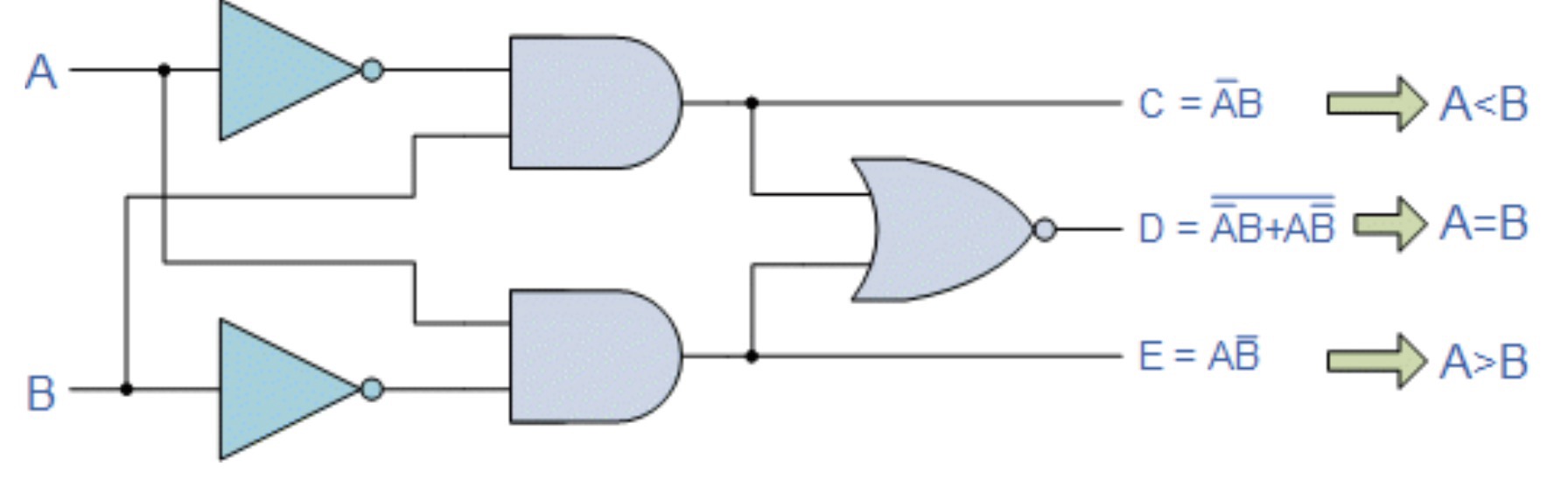
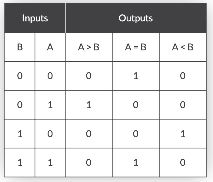
Design a circuit that compares 1-bit number, A and B
- Three outputs:
- G (“Greater”) should be 1 only when A > B
- E (“Equal”) should be 1 only when A = B
- L (“Lesser”) should be 1 only when A < B
Truth Table
Sum of Product
- G:
- E:
- L: